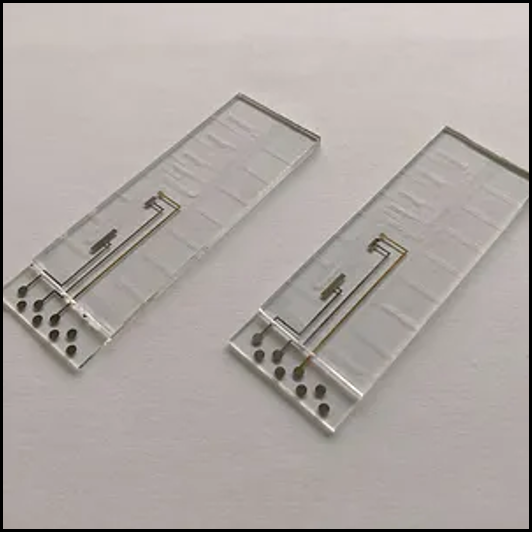
Our customized microfluidic glass chips are manufactured in cleanroom thanks to a photolitography process coupled to a wet etching in a HF based solution.
Moreover, our glass microfluidics chips are sealed thanks to a low-thermal bonding process, with temperatures below 300°C. This process was developed and patented during the PhD thesis of Clément Nanteuil, the CEO of Klearia, in 2010.
Coupling photolitography with wet etching process offer a large range of design’s customization with an ideal roughness and flatness for applications requiring optical observations through a microscope like life sciences for example.
Lower temperatures reduce the risk of damaging sensitive materials or components embedded within the chips, making the process suitable for a wide range of applications involving sensors and actuators. Ideal for the manufacturing of Lab-on-chips.

EXCLUSIVE WEBINAR IN ENGLISH 👉 CLICK HERE TO REGISTER We are excited to invite you…

Skinobs Revamps “We Are Testing” with a bold new identity and website ahead of NYSCC…

👉 The Skinobs team will be delighted to welcome you booth 857, to talk with…